 Let’s start out with a widely-unknown piece of information: the first ever printed circuit board was created in 1936 by Mr. Paul Eisle. However, its application didn’t find any ground until the US Defense Industry started incorporating PCBs in their bomb detonator systems in the 1950s. Conversely, things are over and above different today as PCBs are integrated in almost all the electronic devices we see around every day. From consumer electronics to aerospace, new energy, automobile and personal computers, you name it and it’s there.
PCB fabrication process refers to the assembling of circuit boards in devices so that they can be made of use. To learn more about this process, keep reading below:
 PCB Fabrication Process
Primarily, PCB fabrication takes place in a PCB fab house using two types of software. First of all, Computer Aided Design (CAD) is utilized to design the electronic illustration of the circuit that is to be produced. Once the design is produced, the Computer Aided Manufacturing (CAM) is deployed by skilled and professional engineers to produce the prototype of printed circuit boards.
Step#1
Once you achieve the prototype design, the first step is to select the material of the PCB. There are several different kinds of PCB materials available in the market, the most popular ones being Alumina, Arlon, Bakelite, Ceramic, Polyimide etc. Make sure it exudes the dimensions of the printed circuit board.
Step#2
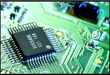
 Upon the selection of the material, the first step is applying a copper coat over the entire board. Using a photosensitive process, the layout of the circuit is printed on the board. Then, the additional copper is eradicated from the sides of the board using the photo engraving process. The copper that’s left on the board is used to carve the tracks and traces of the PCB circuit.
There are two processes used for connecting the traces of the circuit. In the first process, the CNC machines are utilized to get rid of additional copper. Then, in the second process, a define-resistant printing process is deployed to cover the areas where the traces must be present.
Step#3
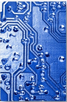
In order to frame the components, holes are drilled (through laser or other drill bit) into the points where electrical components are fixed on the board. Once the holes are made, hollow nails are inserted and covered with a process of electroplating that produces and allows electricity to flow through the layers of the board.
Step#4
Finally, a shielding material is poured over the board to cover all the parts except for the pads and holes. Then, the board is screen-printed so that the labels form a definitive appearance at existing locations.
If you want to buy printed circuit boards, then Super PCB is the right place for you. We’re one of the finest and high-quality PCB manufacturers in the US, serving all kinds of big and small business clients belonging to diverse industries. Learn more about our capabilities or contact us here.