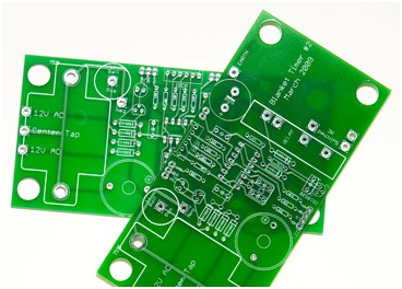
 A PCB (printed circuit board) is a self contained module of interconnected electronic components. PCBs are found in various devices such as computer systems, telecommunications systems, radios, radars and so much more.
The process of making PCBs is complex, long and varied. But despite that, there are some elements of this that all PCBs must go through if effective and functioning products are to be brought out in the end
The Design of PCBs
Each printed circuit board is designed for a unique function. That is why there isn’t a standard layout of PCBs that can be followed. Designers and engineers used computer aided design (CAD) system to make the layout for the PCB. The layout contains the paths for the components, space required and holes that need to be made.
After the circuit pattern has been laid out, a negative image (also called a mask) is printed out on a clear sheet of the exact shape and size. The areas that are not part of the original circuit pattern are shown in lack on the negative image, while the requisite pattern is shown completely clear.
Raw Materials Needed
The most common substrate used in PCBs is a glass fiber which is actually reinforced fiberglass epoxy resin that has a copper foil bonded to either one or both sides. Printed circuit boards are comprised from paper reinforced phenolic resin. With a bonded copper foil, they are quite in expensive and are frequently used in household electrical devices.
The circuits that are printed are made up of copper. This copper is plated (also called etched) to the surface of the substrate to leave the pattern desired.
The copper circuits also need to be coated with a thin layer of tin-lead to stop the process of oxidation. For excellent conductivity, contact fingers are plated (etched) with first tin-lean, then nickel and end with gold.
Additional components are also purchased which include diodes, integrated circuits (IC) chips, resistors, capacitors, transistors, etc.
The Manufacturing Process
The entire processing and the assembly of the printed circuits boards are done in an ultra clean environment. It has to be made sure that the air components are kept completely free of any type of contamination.
A typical two sided printed circuit board goes through the following manufacturing process.
The substrate is made using the glass fiber and epoxy resin which is then ‘baked’ with the copper foil, which in this case acts as an adhesive. Later the panels are all staked together to keep them from moving and holes are drilled out in accordance with the design layout. The non conductive holes are plugged in to keep them from being drilled later on. After this, the circuit pattern is printed on the panel. This process can be both addictive and subtractive. The desired patterns are printed (also called etched) on the panel of removed. Later a solvent is used to reveal the wanted patterns and to dissolves the unwanted ones. Contact fingers are attached and the plating is done first in tin-lead, then nickel and finally with gold. To protect the tin-lead covering the panel is passed through a hot oil bath from which the tin-lead emerges shining and in the end, the panels are cut into the shape they are needed for. If the panels are not to be used immediately, then they are sealed away.
Quality Control
The prepared PCBs have to go through a series of quality control tests to ensure their safety and functionality. If they are found lacking even in a single field then they are taken out of the batch. The boards are later tested for the functional performance to make sure that the output is according to the desired limits. Some boards even have to go through environmental tests to see how factors like heat, humidity, vibration and deep impact will affect them.
PCB fabrication is conducted in such way by companies such as ours to ensure that highest quality PCBs are produced each and every time. For all your PCB production needs you can contact us anytime or call us directly at (214) 550-9837.
