
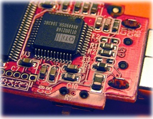
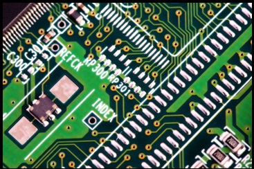
 When it comes to surface mount assembly, stencils provide the classic entry precise and repetitive deposition of solder paste. Knowing that solder paste is printed through the stencil openings, the deposition allows a solid hold for the components. Moreover, when reflow takes place, it sturdily secures in place over a PCB.
It is the shape, size, thickness and design of the stencil that determines the same for the deposits; this is the most crucial and decisive aspect of the overall high-yield assembly process. There are two basic functions of a solder:
- To ensure accurate placement of material such as solder paste, flux etc;
- To ensure the configuration of properly sized and shaped deposits.
Stated below are the three stencil technologies that are widely being used in the PCB industry today:
1. Laser-Cut Process
This is a subtractive process whereby the Gerber files are translated into a CNC-type language so that it can be easily comprehended by the laser. The opening is cut out by moving the laser head, the table that is holding the stencil or both. The smoothness of the cut made during the process are dependent on a number of factors such as speed, size of the beam spot, power of the laser and beam focus. This process is capable of making very precise apertures over a range of shape and size specifications. Many times, electro-polishing and nickel-plating are used to make the surface walls smooth.
2. Chemical Etching
During this process, metal mask and flexible metal mask are etched through chemical milling from both sides using two positive images. The etching does not only proceed in the standard vertical direction, but also in a lateral direction. This is also referred to as undercutting whereby the openings are larger, facilitating additional solder deposition. While it’s hard to obtain smooth walls through this process, electro-polishing can be used make the walls smooth. Moreover, nickel-plating can also be used for the same purpose as it enhances the regularity and efficiency of the printing performance.
3. Electroformed Stencil
 This technology was introduced during the mid 90s. While the aforementioned two technologies are subtractive, electroformed process is an additive one. During this process, the opening is formed by electroplating the nickel on a mandrel consisting of photo-resist pillars figured on the surface. So, each pillar forms an aperture when the nickel is plated up to reach the required amount of stencil thickness. Once the photo-resist dissolves, the stencil is peeled away, leaving behind smooth aperture walls. Here, the post-processing methods of electroplating and nickel-plating are not required.
At Super PCB, we provide an array of high-quality printed circuit board services that range from rigid PCB fabrication to stencils and a lot more. Learn more about our capabilities or make an online PCB quote here.